PCB Design & Assembly
Full in-house PCB schematic design, layout, and PCBA services delivered by experienced Singapore engineers. From rapid prototypes to production-ready assemblies.
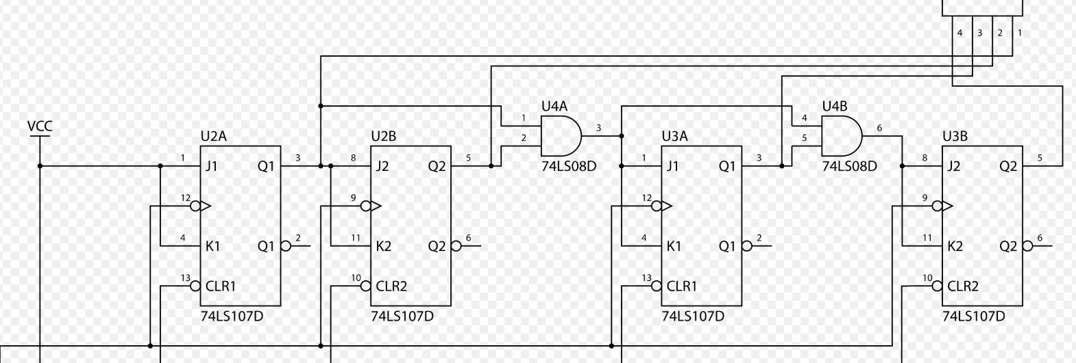
Schematic & Layout Design
Our experienced PCB design engineers deliver professional schematic capture and layout design services using industry-leading CAD tools. We specialize in complex, high-density designs that meet the most demanding specifications.
From single-layer boards to multi-layer high-frequency designs, we handle rigid, flex, and rigid-flex PCBs for applications spanning consumer electronics to aerospace and medical devices.
- High-speed digital and analog design expertise
- Signal integrity and impedance-controlled routing
- DFM and DFT optimization for manufacturability
- EMC/EMI compliance design considerations
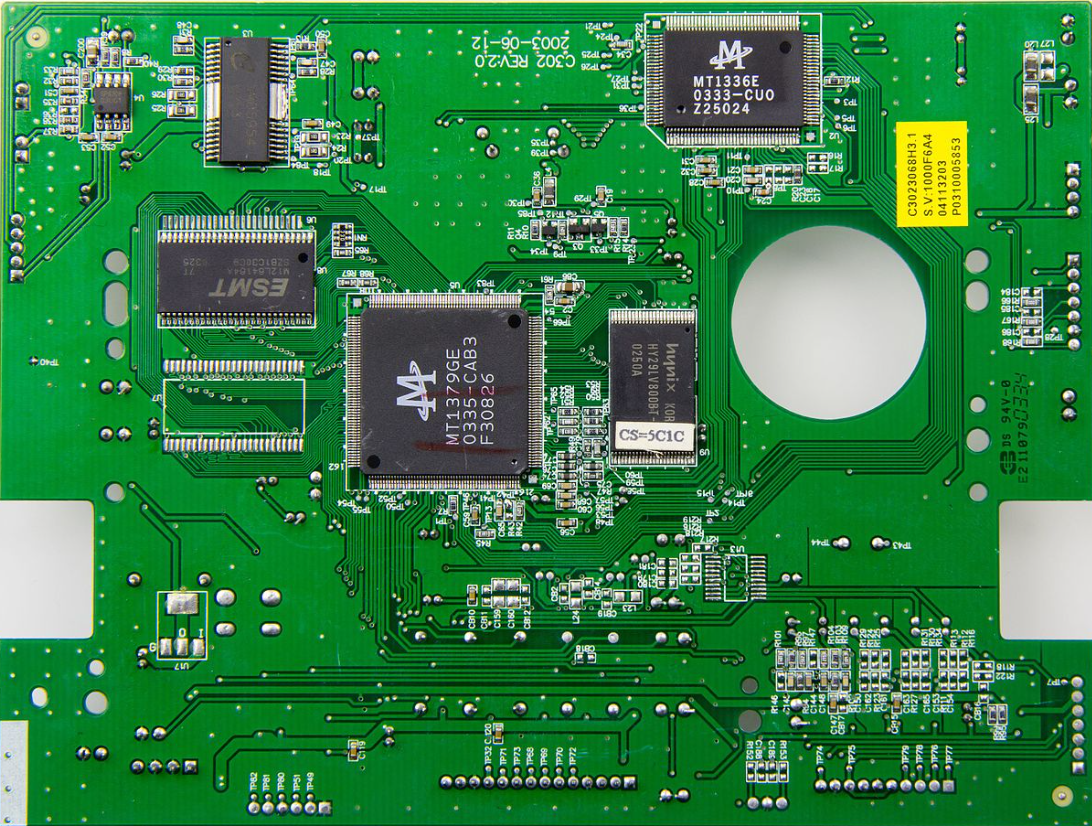
PCBA Assembly Services
Our assembly capabilities cover the full spectrum of PCB manufacturing requirements. We work with trusted fabrication and assembly partners to deliver consistent, high-quality results with competitive lead times.
Whether you need quick-turn prototypes for development validation or production volumes for market deployment, we ensure every board meets rigorous quality standards.
- SMT and through-hole assembly
- BGA, QFN, and fine-pitch component placement
- Lead-free and RoHS-compliant processes
- Conformal coating and potting services
Our PCB Services
Comprehensive solutions from concept to production, backed by rigorous quality assurance at every stage.
Schematic Design
Professional circuit design with component selection, power distribution analysis, and signal integrity optimization.
Layout Design
Multi-layer PCB layout including HDI, high-frequency, rigid-flex, and impedance-controlled designs.
Prototype Fabrication
Quick-turn prototype boards for design validation and testing, with expedited delivery options available.
SMT Assembly
Surface mount technology assembly with automated pick-and-place for consistent, high-quality results.
Through-Hole Assembly
Manual and wave soldering for through-hole components, connectors, and mixed-technology boards.
Testing & Inspection
Comprehensive ESS, FAT, and functional testing with AOI and X-ray inspection capabilities.
Design Capabilities
Start Your PCB Project Today
Share your requirements with our engineering team and receive a detailed proposal within 48 hours.
Request a Quote